For available material grades, dimensions and machining options, see our Aluminum Nitride (AlN) Substrates product page.
1. Start with the thermal resistance budget
Aluminum nitride substrate selection begins with the allowable temperature rise, device power loss and heat-flow path. Establish how much thermal resistance the ceramic layer can contribute after accounting for die attach, metallization, interfaces and the cooling structure.
For steady, one-dimensional conduction through a uniform layer:
Rth = t / (k × A)
Here, Rth is thermal resistance in K/W, t is thickness in metres, k is thermal conductivity in W/(m·K), and A is the cross-sectional heat-transfer area in m². The temperature difference across this layer is ΔT = Q × Rth, where Q is the heat passing through it in watts.
Use this relationship to compare candidate designs. A small heat source on a larger substrate introduces lateral heat spreading, so neither the full substrate area nor the device footprint should automatically be treated as a uniform conduction area. Final temperature predictions require an appropriate thermal model or measurements on the assembled device.
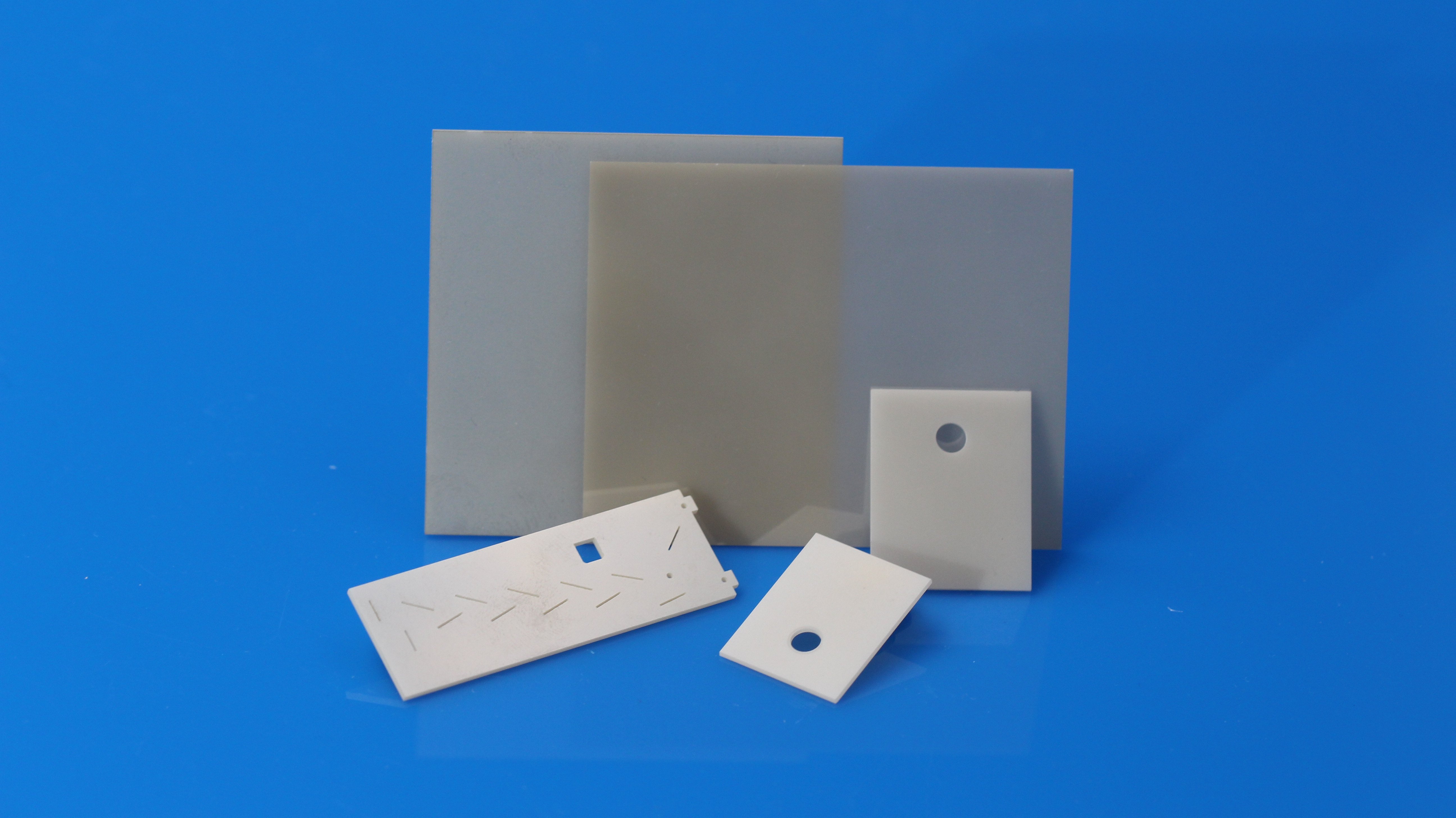
Aluminum Nitride Substrate Selection Guide: Thermal Conductivity, Thickness, Surface Finish and Qualification
2. Selecting the Right Thermal Conductivity Grade
Compare 170, 200 and 230 W/(m·K) grades under the same geometry and boundary conditions. The higher grade is valuable when the ceramic layer makes a meaningful contribution to total thermal resistance; its benefit is smaller when interfaces or the cooling structure dominate.
| Grade | When to evaluate it | Decision criterion |
|---|---|---|
| 170 W/(m·K) | Initial option where thermal, insulation and cost requirements must be balanced. | Does the complete assembly meet the temperature limit with adequate design margin? |
| 200 W/(m·K) | The geometry is fixed and a moderate reduction in ceramic-layer resistance is useful. | Does the calculated improvement justify the change in material cost? |
| 230 W/(m·K) | Thickness cannot be reduced and the thermal budget requires lower ceramic-layer resistance. | Confirm the benefit at the actual heat-source area, operating temperature and interface quality. |
For a 0.55 mm ceramic layer and an assumed uniform heat-transfer area of 10 × 10 mm, the calculated comparison is:
| Conductivity | Rth | Reduction from 170 W/(m·K) |
|---|---|---|
| 170 W/(m·K) | 0.0324 K/W | Reference |
| 200 W/(m·K) | 0.0275 K/W | 15% |
| 230 W/(m·K) | 0.0239 K/W | 26% |
These are calculated values, not measured assembly results. A 26% reduction applies only to the ceramic layer in this model. If that layer contributes 20% of total thermal resistance, the idealized reduction in total resistance is about 5.2%, with all other resistances unchanged.
Specify the test temperature, method and minimum acceptance value separately from the grade name. For the 170 W/(m·K) material, the reference specification is ≥170 W/(m·K) at 25 °C, with a typical value of 175 W/(m·K). The reference relative permittivity is 8.7 at 1 MHz and 25 °C. These values should not be transferred automatically to other grades. For elevated-temperature designs, obtain temperature-dependent data or validate thermal performance under operating conditions.
3. Select thickness together with insulation and manufacturability
At constant conductivity and area, ceramic-layer resistance is proportional to thickness. Reducing thickness from 0.635 to 0.38 mm reduces this resistance by approximately 40%. This can be a useful alternative to changing conductivity grade, provided the thinner part meets electrical and mechanical requirements.
A thinner substrate also changes handling, clamping, singulation and assembly conditions. Check support span, hole and edge geometry, metallization stresses and damage during transfer. Material dielectric strength alone does not establish a safe operating voltage: electrode geometry, insulation distances, voltage waveform, test duration and the assembled insulation system must also be evaluated.
Choose the panel format around the downstream equipment and usable area. A 138 × 190 mm production panel can be a starting point, but the best layout depends on edge exclusions, tooling features and cutting allowances. Compare cost per accepted finished part, including machining, inspection and yield, rather than cost per panel alone.
4. Define thickness tolerance, TTV, warpage and surface finish separately
| Requirement | What it describes | What to specify |
|---|---|---|
| Thickness tolerance | Deviation from nominal thickness. | Nominal value, tolerance and measurement locations. |
| Total thickness variation (TTV) | Maximum minus minimum thickness on one substrate over a defined area. | Limit, edge exclusion, point distribution and measurement method. |
| Warpage / flatness | Departure from the agreed geometric reference. | Definition, datum or support condition, measurement area and units; define the reference length for percentage warpage. |
| Surface roughness | Texture characterized by an agreed parameter, such as Ra. | Required side, locations, measurement direction, instrument method and filtering/cutoff conditions. |
| Local defects | Pits, scratches, particles, chips or other localized damage. | Functional zones, defect limits and inspection conditions. |
These requirements are not interchangeable. A substrate may meet its overall thickness tolerance yet fail a TTV requirement. A low Ra value does not prove that the chip-attach area is free of pits or contamination. Measurements across different pieces cannot establish the TTV of an individual piece.
Select as-fired, ground, lapped or polished surfaces according to the next process. Grinding can control thickness or geometry without necessarily producing a smoother surface than the as-fired condition. Mark circuit, die-attach and bonding areas on the drawing so that local acceptance criteria match the actual function. Evaluate bare and metallized substrates separately, because subsequent processing may change their shape.
5. Match the substrate to the downstream process
| Process | Selection priorities | Validation focus |
|---|---|---|
| DPC metallization | Surface condition, cleanliness, geometry and via quality where applicable. | Metal adhesion, circuit integrity and shape after metallization. |
| Thick-film circuits | Compatibility with the selected paste, printing conditions and firing profile. | Pattern quality, adhesion, electrical results and distortion after firing. |
| Thin-film and precision optoelectronic packaging | Local surface quality, TTV, flatness and attachment requirements. | Film continuity, alignment, bond quality and assembly thermal performance. |
No single roughness value qualifies a substrate for every metallization system. Establish acceptance limits using the intended metal stack, paste or bonding process. Keep the supplied condition explicit: bare ceramic and a metallized circuit require different inspection scopes.
For further DPC-specific discussion, see How to Qualify AlN Substrates for DPC Metallization. Set the final acceptance criteria against your own qualified process.
6. Use representative test data without turning it into a blanket guarantee
The following representative results relate to a nominal 100 × 100 × 0.55 mm substrate format in the 230 W/(m·K) grade. They illustrate a combination of measured properties; they do not define the acceptance limits for every order.
| Property | Recorded range | Reported mean |
|---|---|---|
| Thermal conductivity | 230–231 W/(m·K) | 231 W/(m·K) |
| Flexural strength | 352–440 MPa | 392 MPa |
| Density | 3.27–3.28 g/cm³ | 3.28 g/cm³ |
| Surface roughness | 0.445–0.485 μm | 0.470 μm |
| Length | 100.03–100.04 mm | 100.04 mm |
| Width | 99.98–100.00 mm | 99.99 mm |
| Thickness | 0.557–0.563 mm | 0.560 mm |
Density was measured by the vacuum method. Means retain the precision of the underlying test data. The thermal-conductivity test temperature is not specified in the available data, so these results are not presented as values measured at 25 °C. Confirm the full test conditions before using them as a design input or comparing them with other datasets.
The 0.557–0.563 mm thickness range does not establish a TTV of 0.006 mm: the measurement record does not identify a within-piece thickness map. Likewise, the roughness results describe the tested surface condition, not a polished-surface specification. Qualification should use the intended production thickness, surface finish and downstream process.
7. Qualify the material through three stages
| Stage | Evaluate | Retain |
|---|---|---|
| Bare substrate | Dimensions, TTV where required, surface condition and agreed material properties. | Drawing revision, lot identity, measurement methods and results. |
| Downstream processing | Actual metallization, printing, firing or bonding process; adhesion and deformation. | Process settings, inspection results and yield. |
| Assembly | Temperature distribution, insulation and application-relevant reliability tests. | Boundary conditions, acceptance limits and failure observations. |
Use samples from multiple lots before production release where consistency is critical. Fix the material grade, surface treatment, process route and inspection definitions that passed qualification. Agree how changes in material, processing or test methods will be notified and evaluated.
Control handling and storage as part of this process. Protect surfaces and edges, retain lot identification, and qualify cleaning or other pretreatment with the downstream process. An unrecorded change in surface preparation can undermine an otherwise valid qualification.
8. Turn the design decision into a purchasing specification
| Item | Required definition |
|---|---|
| Application | Power loss, operating temperature, insulation requirements and cooling arrangement. |
| Material | Conductivity grade, minimum acceptance value, test temperature and method. |
| Geometry | Drawing revision, dimensions, tolerances, holes, slots, TTV and warpage where required. |
| Surface | Required side or sides, finish, roughness measurement conditions and functional-zone defect limits. |
| Supply condition | Bare or metallized; panel or finished part; packaging and handling requirements. |
| Inspection | Sampling, frequency, pass/fail criteria, lot traceability and required report content. |
| Volume and changes | Sample quantity, production forecast, delivery milestones and change-notification requirements. |
Distinguish periodic material characterization from routine shipment inspection. A certificate of analysis (COA) should make clear which results were measured for the delivered lot and which are based on periodic testing. If thermal conductivity or another property must be measured for each lot, agree the sampling plan and method before ordering.
The approved purchasing specification should reflect the design that passed qualification. This gives engineering and purchasing a common basis for comparing quotations, accepting deliveries and managing future changes.