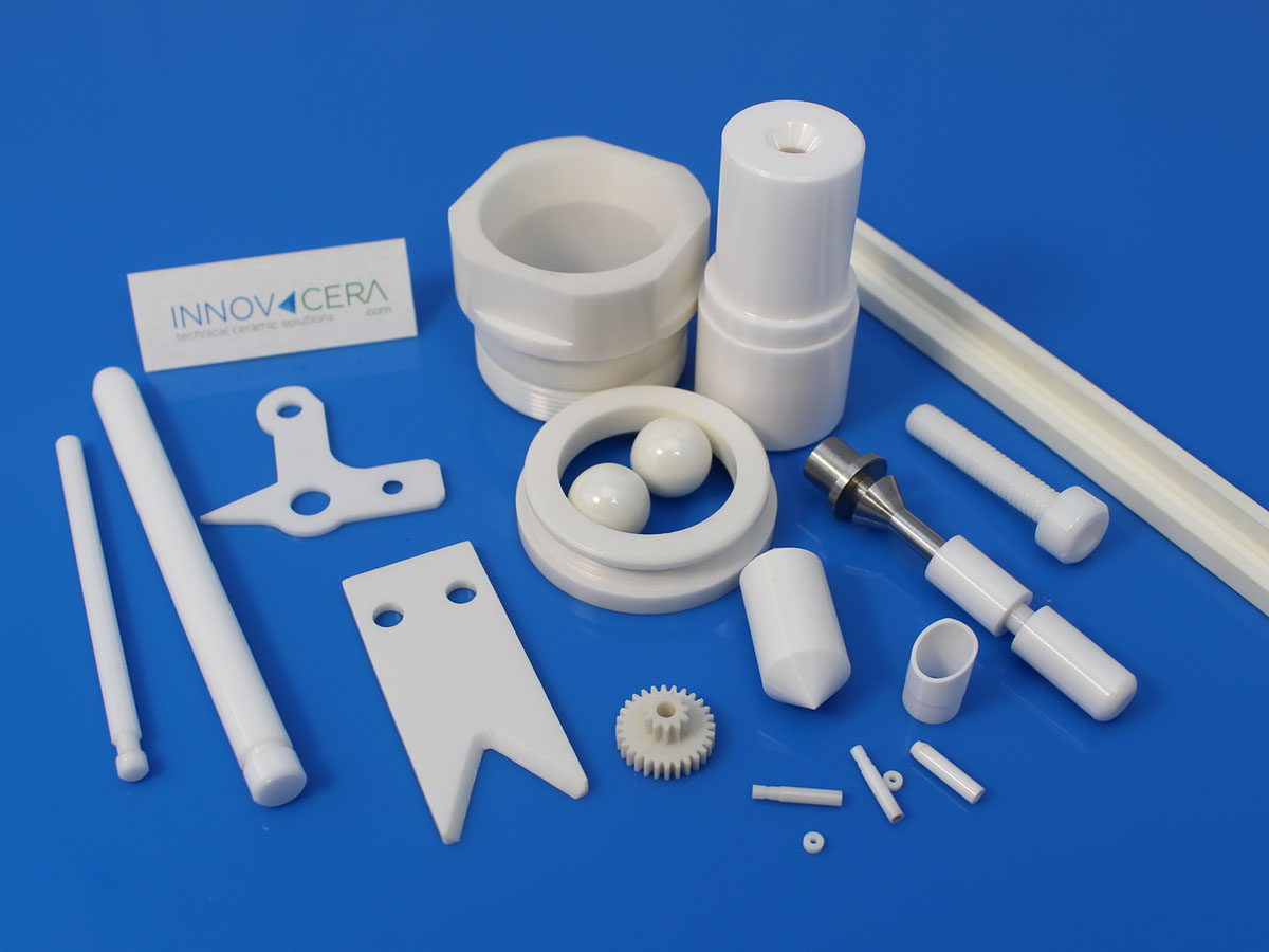
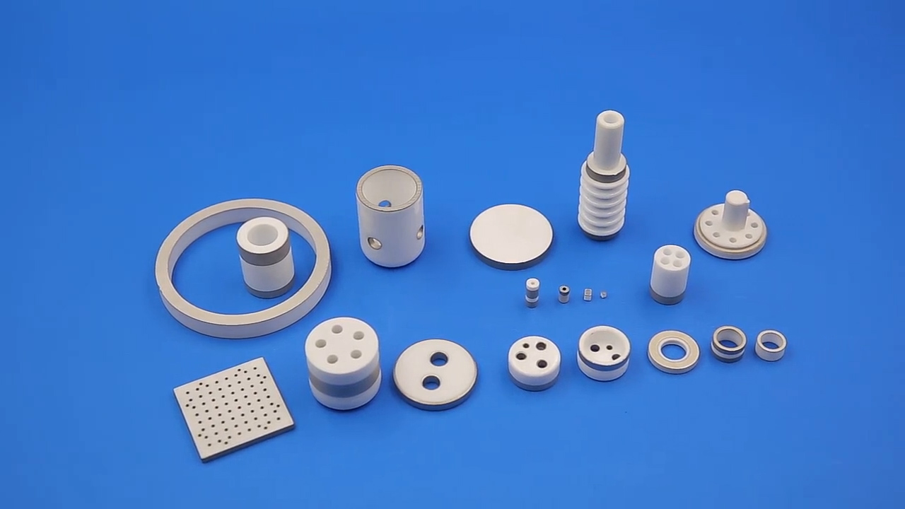
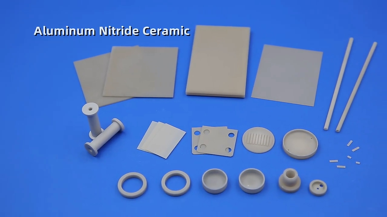
Innovacera Laser Ceramics Products
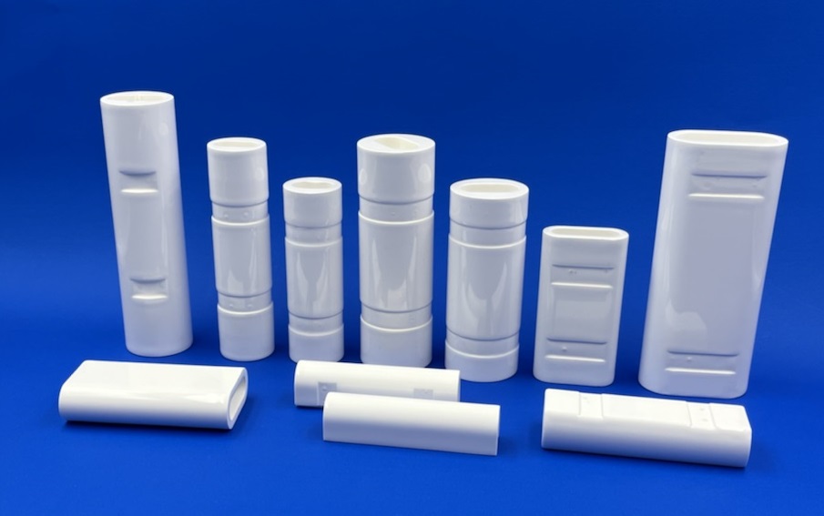
Innovacera provides a series of Laser Ceramic Products. Including a variety of lamp-pumped ceramic cavities for laser welding machines, laser cutting machines, laser marking and medical industries, ceramic sleeves for optical fiber connectors, ceramic rings for laser cutting machines, capacitor filter tubes and other functional ceramic products. And we has the ability to process the small ceramic tube, rod grinding machining, and carry out the research and development and production capacity of brazing connection of ceramic and metal materials. For custom fabrication, you are welcome to inquire!
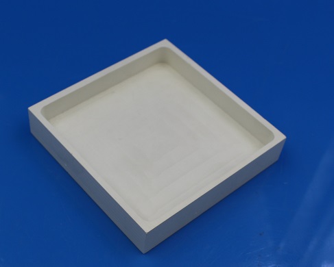
The ceramic reflector green body is made of 99% Al2O3, and the green body is fired at an appropriate temperature to retain proper porosity and proper green strength. The surface of the reflector is fully coated with a high-reflectivity ceramic glaze. Compared with the gold-plated reflector, the biggest advantage lies in its extremely long service life and diffuse reflection.
Main features:
- Dimensional tolerance in height direction can achieve a tolerance ≤1.0mm, other dimensional tolerances can reach ≤0.5mm
- The surface is fully glazed to achieve maximum reflectivity and is easy to clean
- The reflectivity reaches 97% at the wavelength of 600-1000nm
- The reflectivity exceeds 95% in the wavelength range of 380-1100nm
- The body has proper porous and high-strength characteristics
Main physical characteristics:
Color: White
Density: 3.1Mg/m;
Porosity: 22%
Flexural strength: 170Mpa
Thermal expansion coefficient:
7.9×10⁻⁶/С(200~500℃)
9×10⁻⁶/С(200~1000℃)
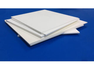
Alumina Laser Ceramic Reflector
The yellow-glazed ceramic concentrating cavity exhibits high reflectivity in the main absorption band of the solid-state laser, and at the same time exhibits the function of reducing the reflectivity in the ineffective absorption band. In contrast, the diffuse reflective ceramic condenser cavity has high reflectivity in the non-absorptive ultraviolet band of the laser crystal, but it cannot effectively filter out the ultraviolet light that produces a harmful color center to the laser crystal. The highly reflective, UV-absorbing ceramic glaze can obviously improve the shortcomings of ordinary ceramic condenser cavities. It has the characteristics of strong laser radiation resistance, high insulation, corrosion resistance, easy cleaning, and UV absorption.
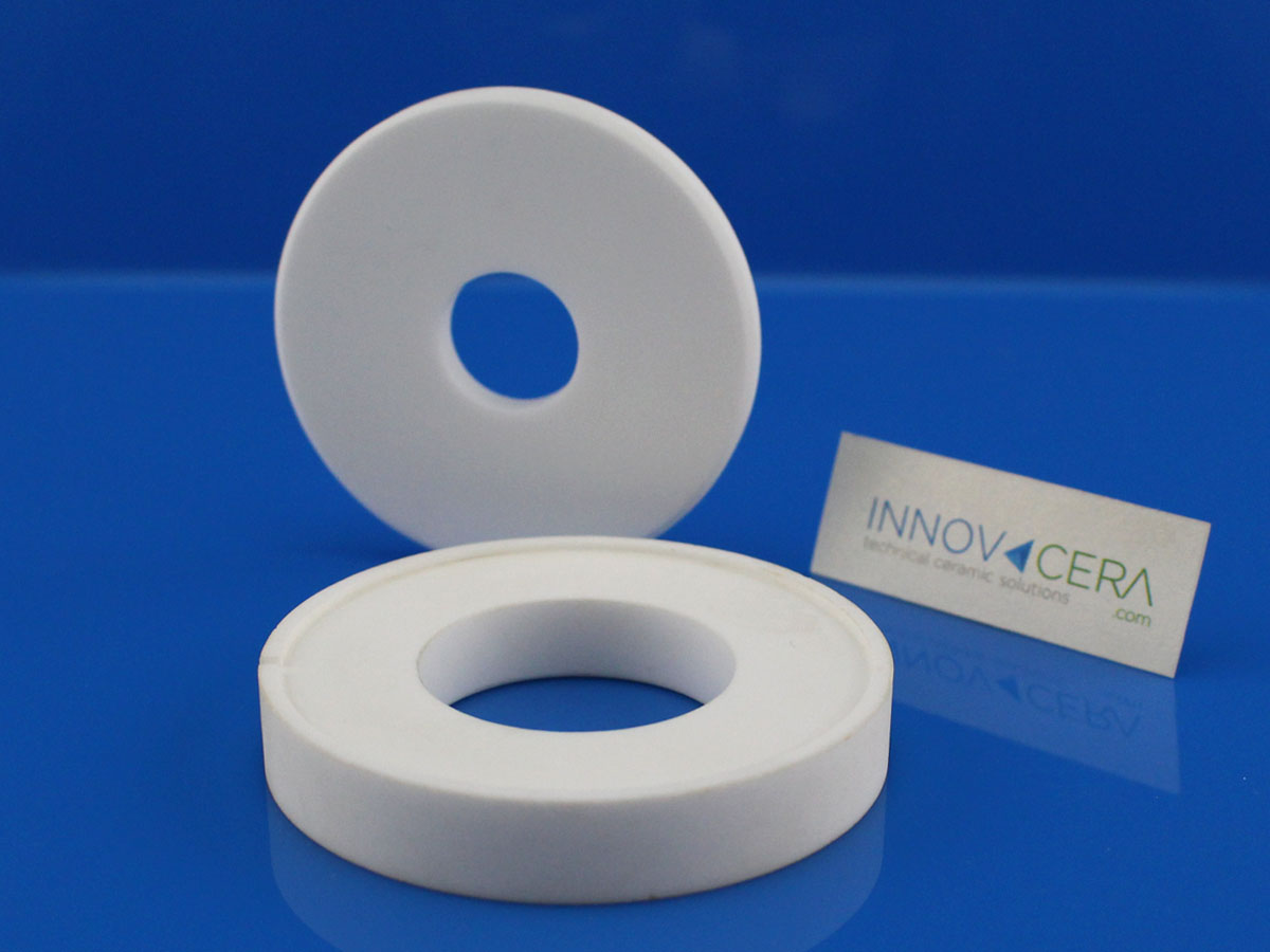
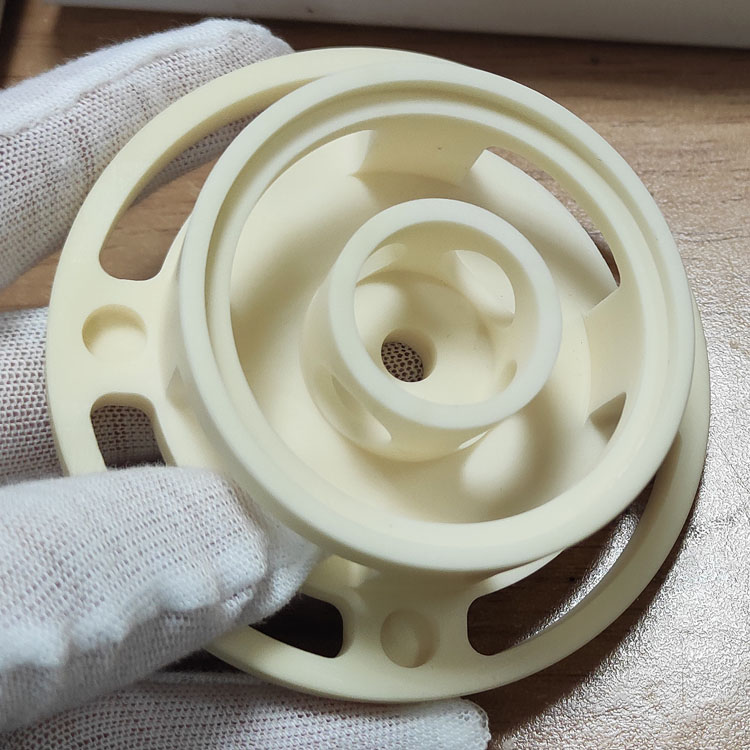
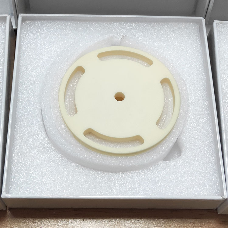
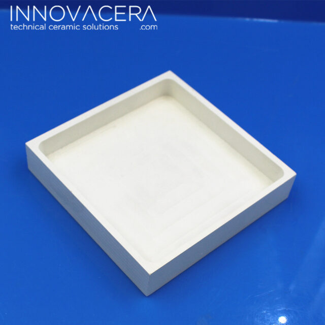
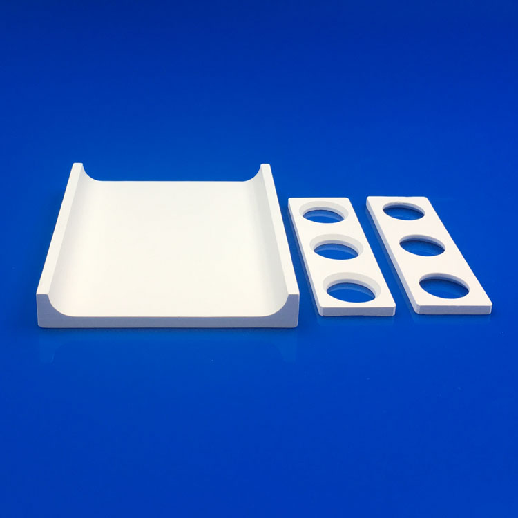
Laser Ceramic Ring
The material is made of machinable glass-ceramic, machined. It has the characteristics of high dimensional accuracy.
machinable glass ceramic parts
machinable glass ceramic ring
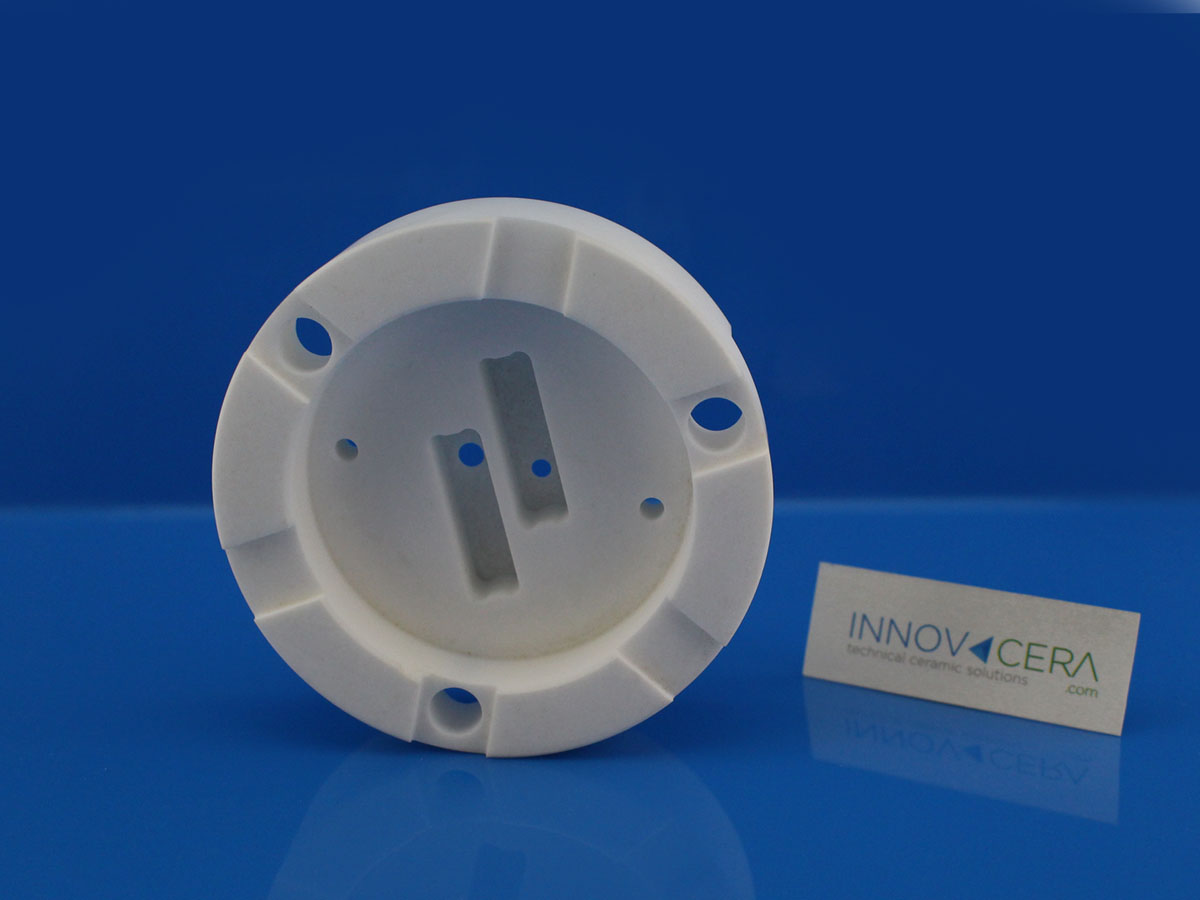
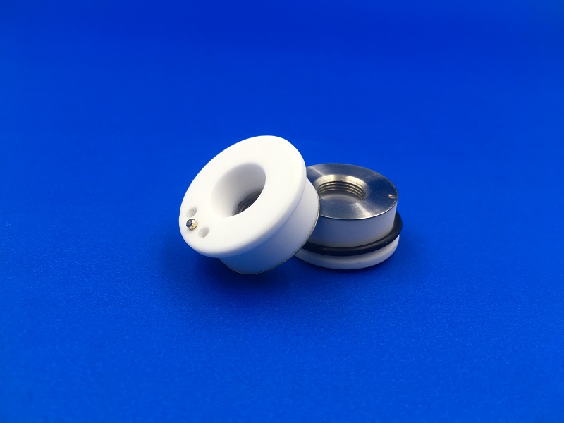
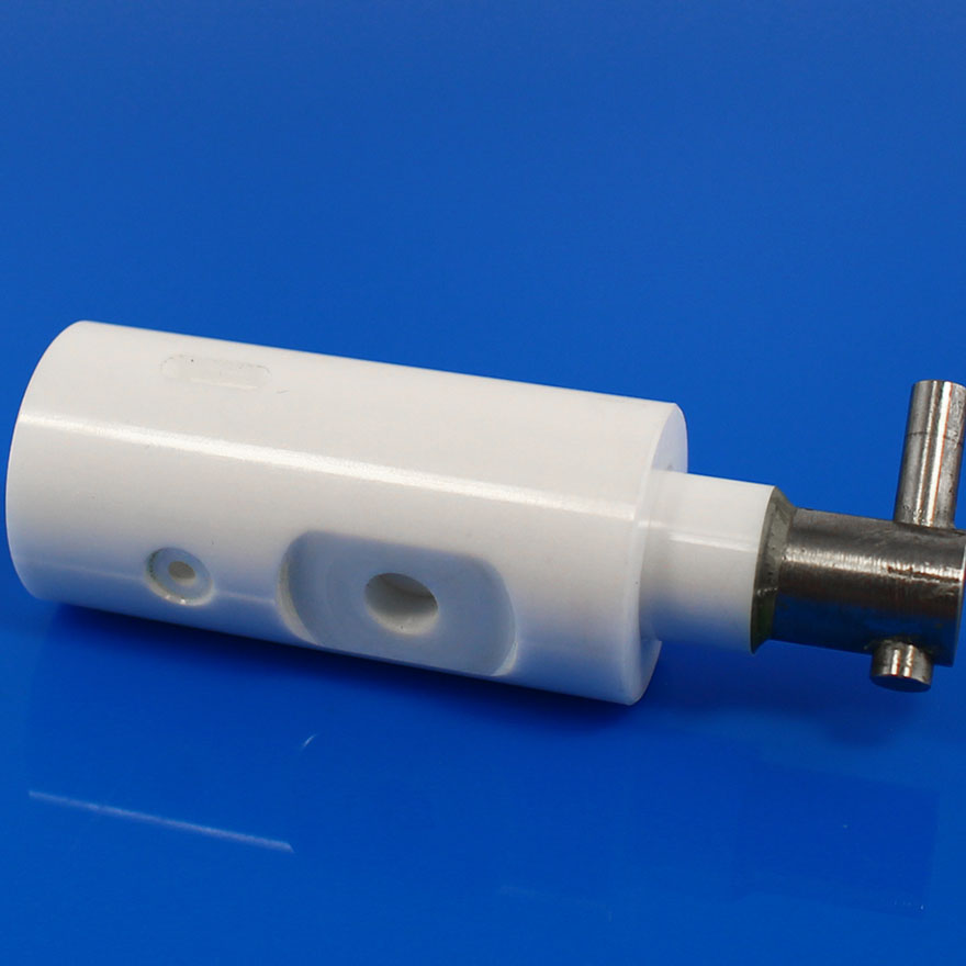
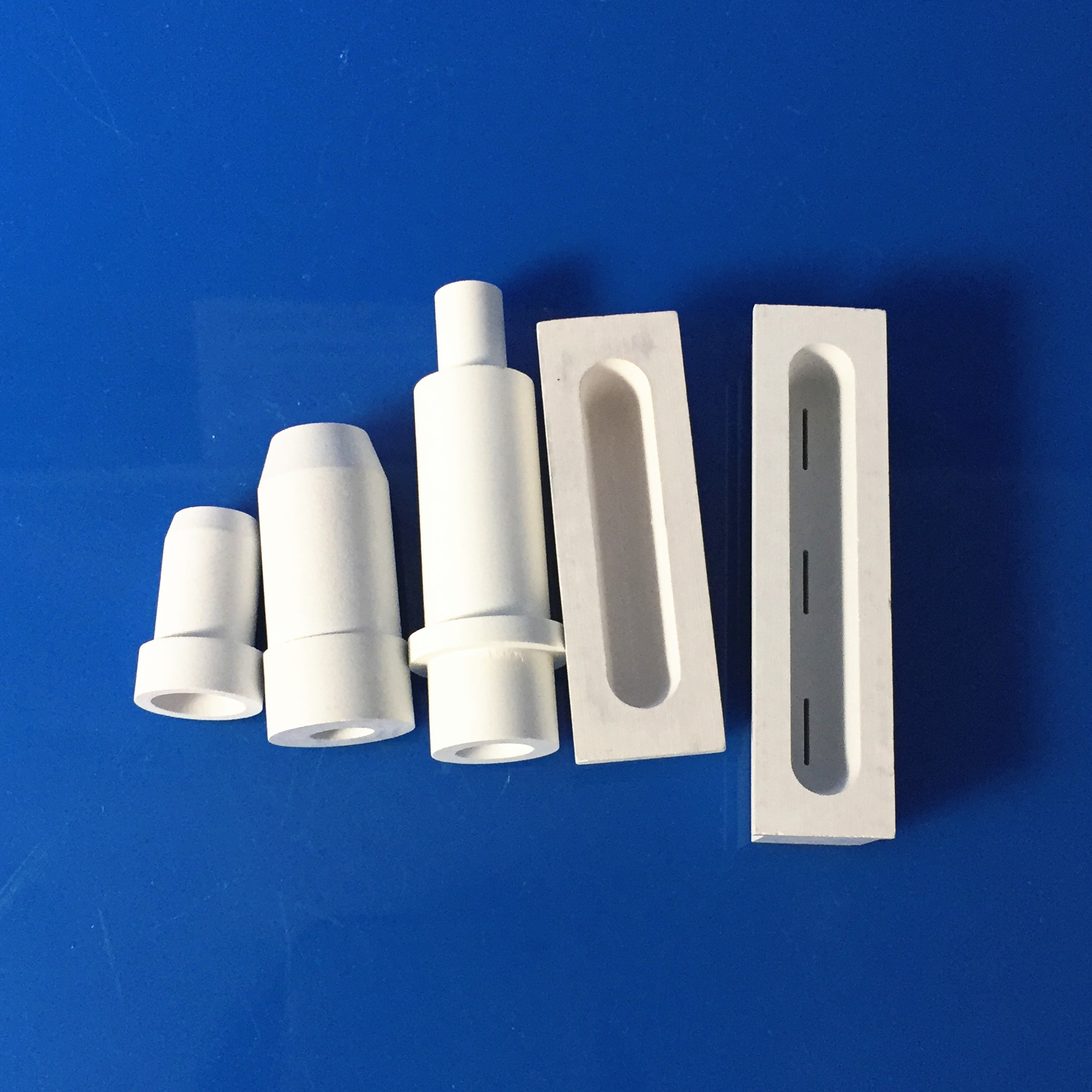
Laser Ceramic Nozzle Holder
The porcelain body is made of imported materials, with high dimensional accuracy and moderate strength. When the workpiece hits the cutting head, it can effectively protect the cutting head.
The hole in the porcelain body adopts a tapered structure, which is conducive to the concentrated spray of compressed air.
The thickness of the bottom plate of the stainless steel connector is 0.3mm, and the induction and cutting speed is fast.
The stainless steel connecting piece and the ceramic body are connected by thread, and the bonding adopts imported high-temperature resistant glue, so the stainless steel piece is not easy to loosen or fall off.
The connecting wire adopts gold-plated copper needles, and the electric signal transmission resistance is small.
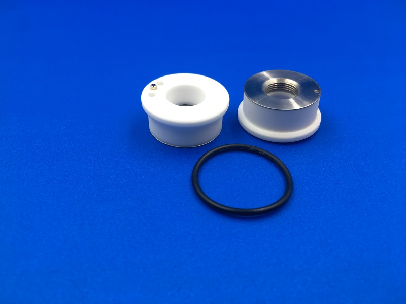
Alumina Ceramic Laser Ring
Ceramic Laser Ring
Standard parts are available in stock, please contact if you need.
For ceramic custom fabrication, you are welcome to inquire!

 Enquiry