Aluminum Nitride Materials Used As Heat Resistant Material
Aluminum nitride materials can be used as high-temperature insulating parts because of their excellent insulating properties and thermal stability.
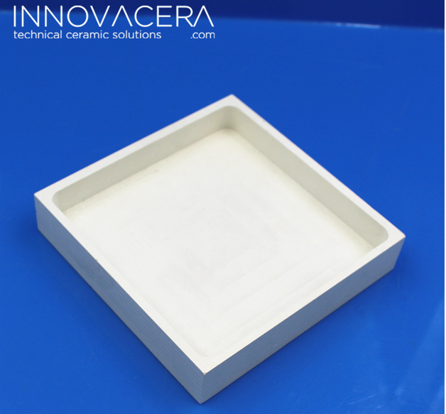
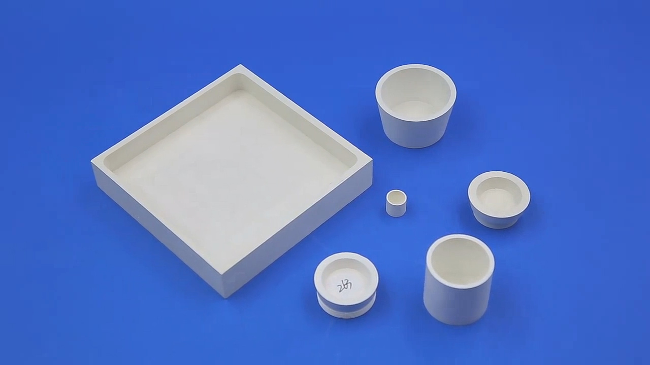
In addition, aluminum nitride and metals such as aluminum, copper, silver, and platinum and semiconductor materials such as gallium arsenide are difficult to infiltrate. It is suitable for crucibles, thermocouple protection tubes, and sintering utensils, and can also be used as containers and treatment of corrosive substances. device.
In addition, aluminum nitride is very stable to molten salt, and it is expected to be used as a high-temperature gas turbine for corrosion-resistant parts such as magnetic fluid power generation (MHD). Since aluminum nitride has a low vapor pressure in a vacuum and is not easy to volatilize at high temperatures, it can be used as an evaporator such as gold.
Aluminum nitride is very stable up to 2000°C in a non-oxidizing atmosphere, so it can be used as an aggregate of refractory materials used in a non-oxidizing atmosphere.
Below is the properties of Aluminum Nitride materials:
| Chemical formula | AlN |
| Color | Gray |
| Density | 3.3 g/cm 3 |
| Thermal conductivity | 160 ~ 190 W/m. K |
| Thermal Expansion ( x10 -6 / ℃ ) | 2-3.5 |
| Dielectric strength | ≥17KV/MM |
| Dielectric Constant (at 1MHZ) | 8-10 |
| Loss Tangent (x10 -4 @1MHZ) | 2.0 |
| Volume Resistivity | ≥10^14 ohm-cm |
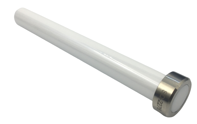
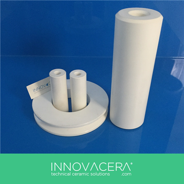
Below is the aluminum nitride crucible we make, any other customized shape could be made. For more information, pls consult with us.

Aluminum Nitride Materials Used As Heat Resistant Material


 Enquiry